Adpt-A16
Overview
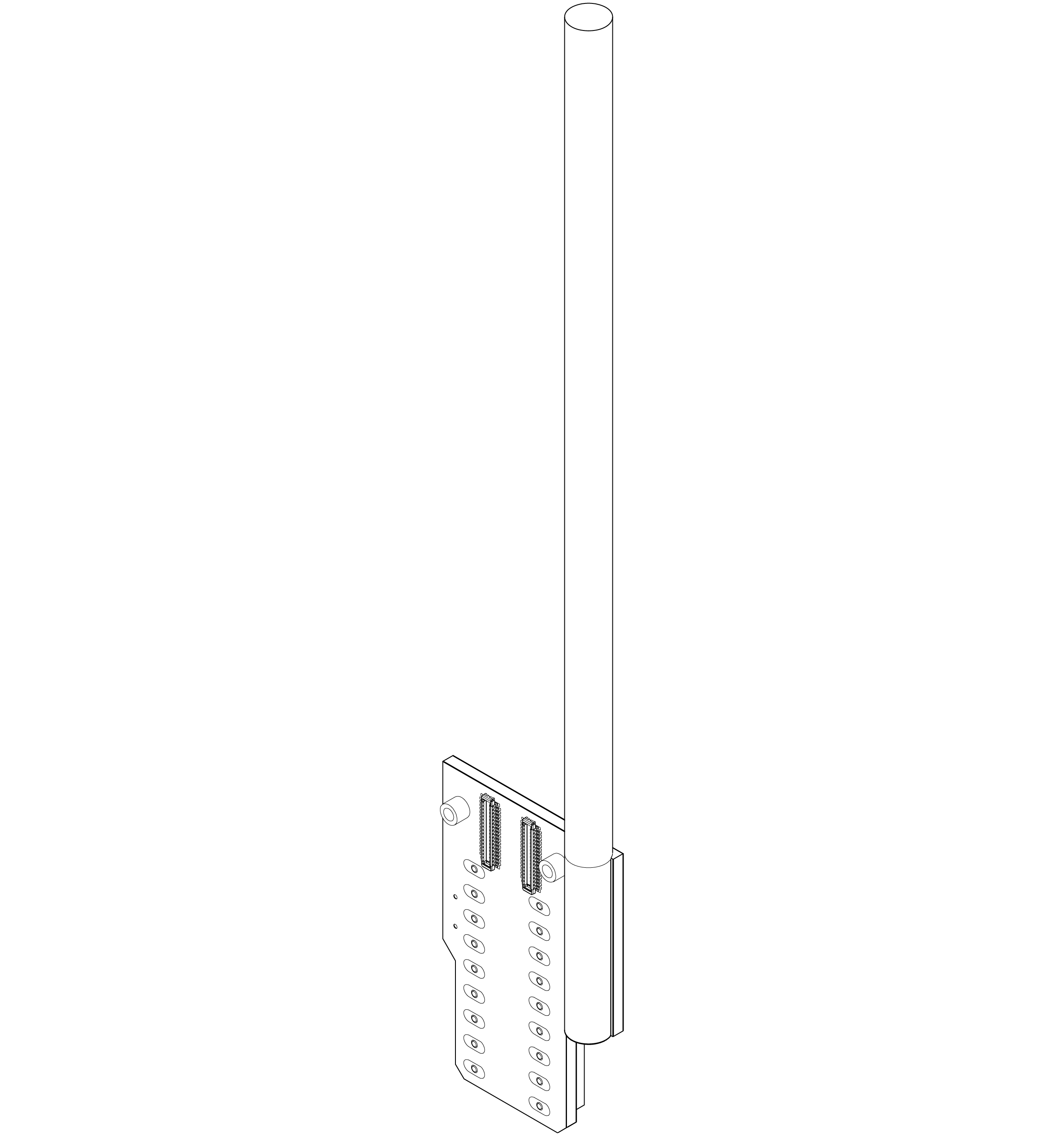
The Adpt-A-series probe adapter enables seamless integration between acute-style neural probes and the X3 X-Headstage™. Designed for versatility, these adapters support 16-, 32-, and 64-channel probes, ensuring broad compatibility with a wide range of neural probes available on the market.
Adpt-A16 Overview
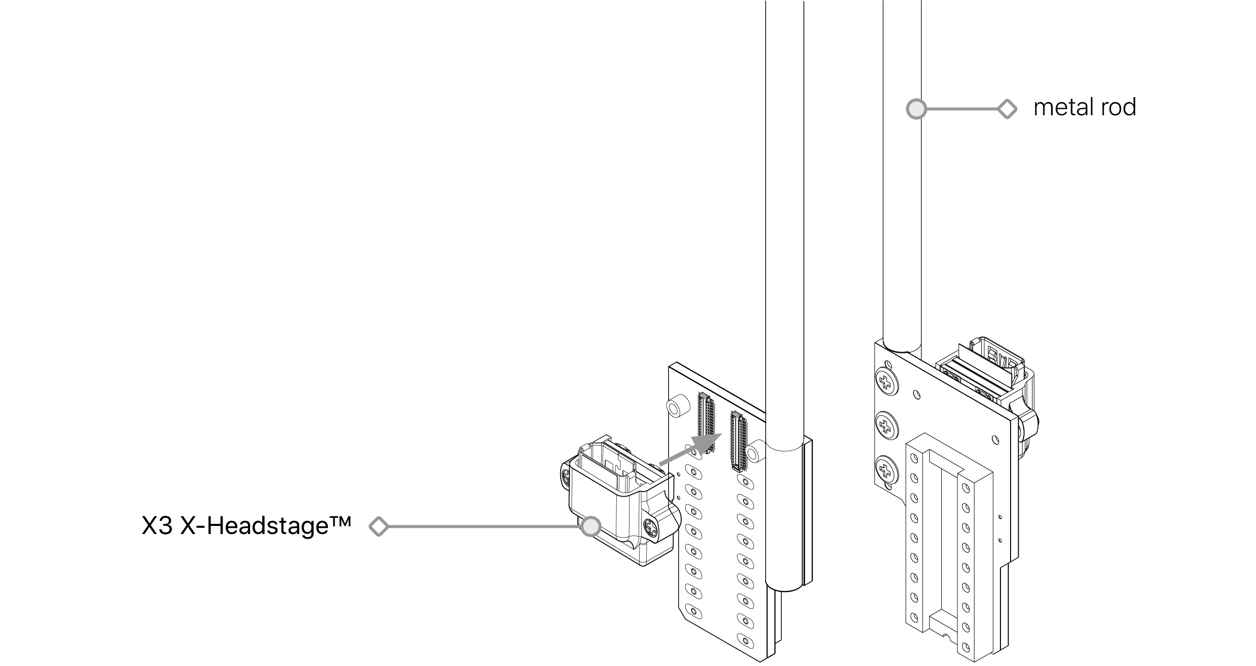
Connector
Headstage
- Molex PN: 505070-3422
Probe
- IC Socket DIP-18P(2x9) 2.54mm/7.62mm
- Compatible Neuronexus probes: A16, D16, MRA16
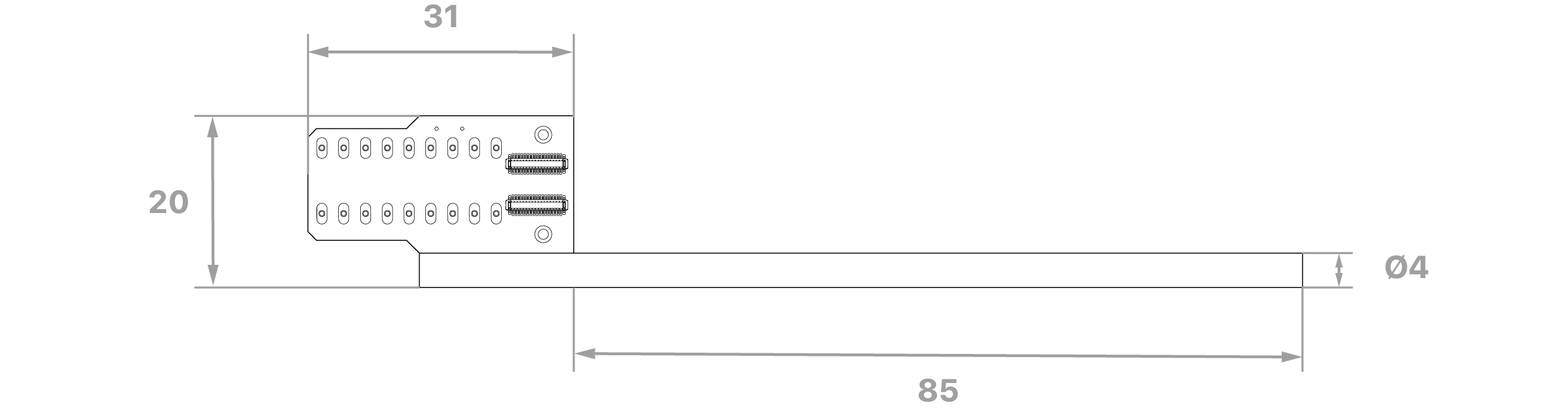
Dimension
V1 & V 1.1
V2
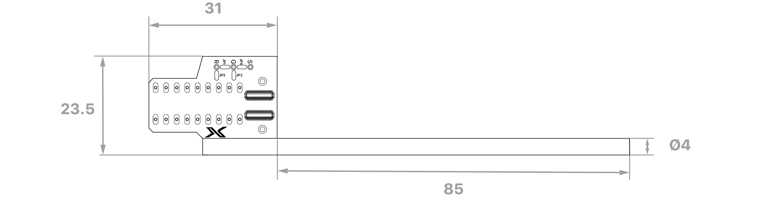
unit: mm
Versions
V1: Identified by K22022 on PCB
Original design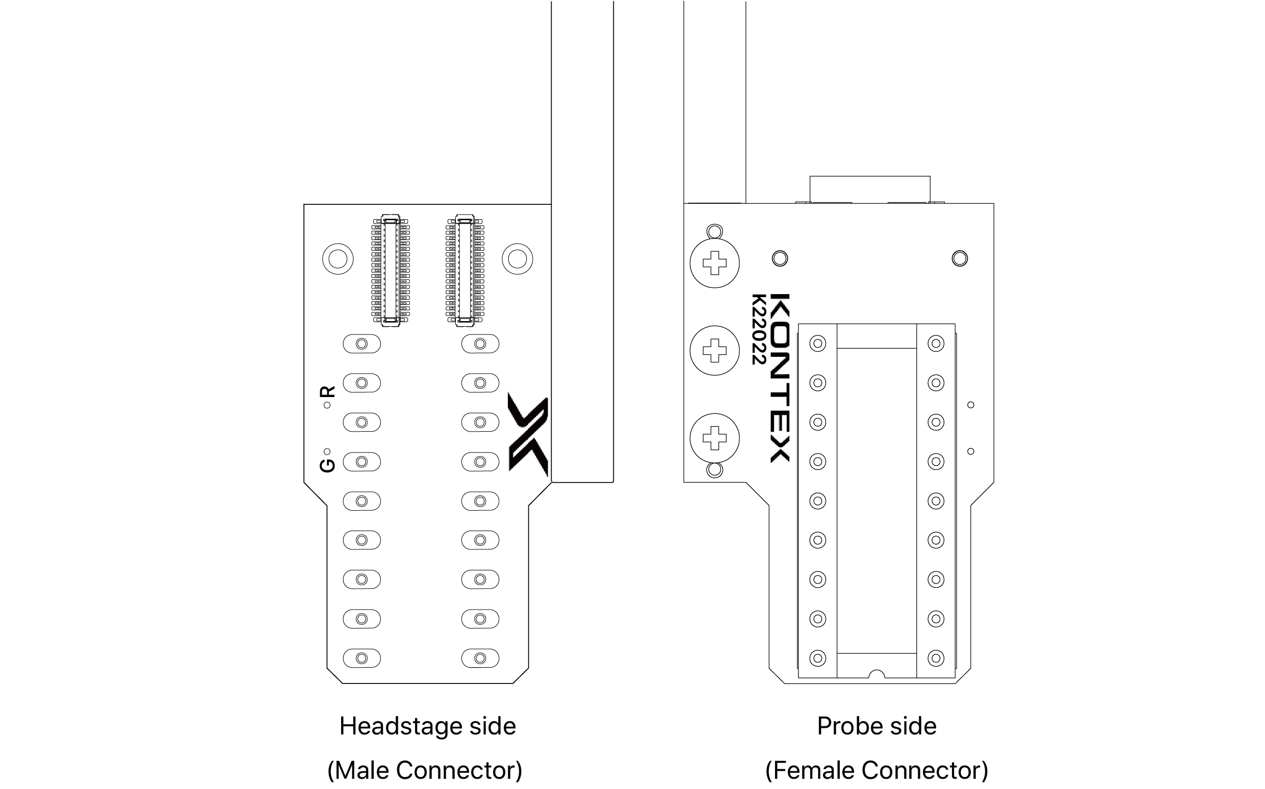
V1.1: Identified by 100011A on PCB

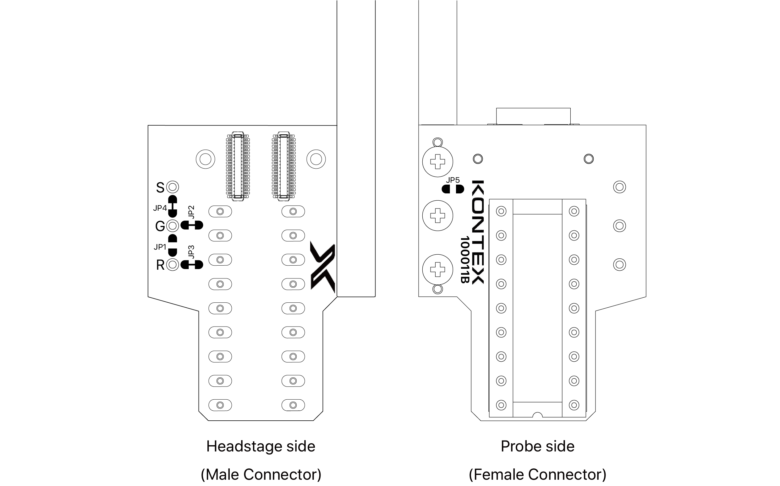
V2: Identified by 100011B on PCB
Ground & Reference Configuration
A16 V1 & V1.1 Adapter (SKU: Adpt-A16v1 & V1.1)
- Ground (G) and reference (R) signals are independent by default.
- To short them together at the adapter, solder a short wire between the G and R pads.
Adpt-A16
A16 V2 Adapter (SKU: Adpt-A16v2)
Proper grounding and referencing are essential for high-quality signal acquisition. Always ensure that both ground and reference signals are securely connected. If either is left floating, significant noise may be introduced into the recordings.
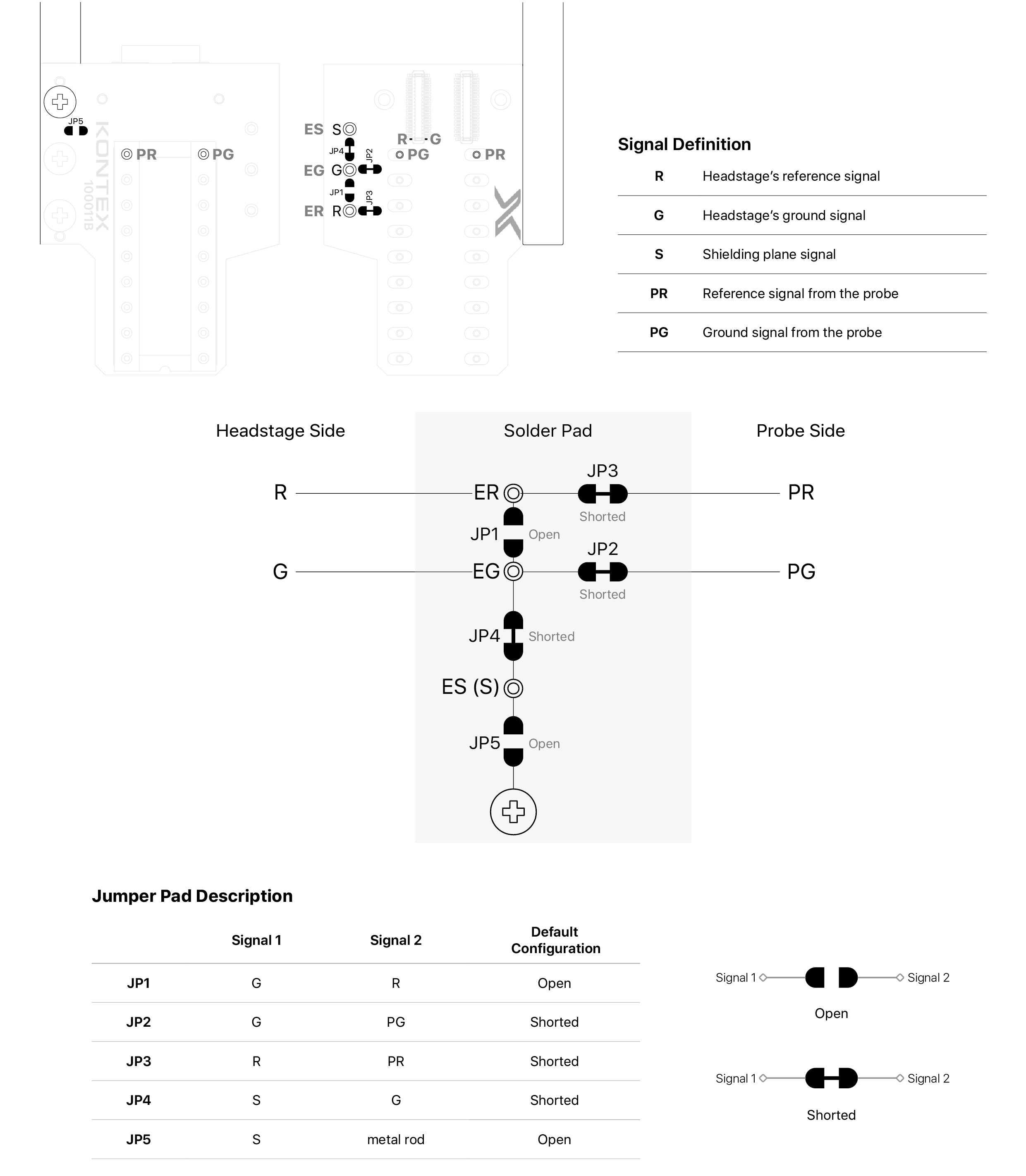
By default, the headstage ground (G) and reference (R) are independent.
- To connect reference and ground at the adapter, short JP1.
- Ground (G) is sourced from the probe ground (PG). To use an external ground (EG) via the adapter, cut JP2 and solder a wire to the EG pad.
- Reference (R) is sourced from the probe reference (PR). To use an external reference (ER) via the adapter, cut JP3 and solder a wire to the ER pad.
- Shielding (S) is connected by default to ground (G). To use an external shielding signal (ES) via the adapter, cut JP4 and solder a wire to the ES pad.
- The adapter’s metal rod is electrically isolated from the headstage. To connect it to the adapter’s shielding, short JP5.
Configuring the Jumper Pad
① To connect the jumper, apply solder around JP1 until a solid solder bead forms.

② To disconnect, use a soldering iron and desoldering mesh to remove the solder bridging the jumper pad.
If the jumper pas has a default short configuration, use a scalpel or precision blade to cleanly sever the trace.
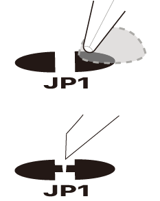
③ After modification, clean the area thoroughly using isopropyl alcohol or flux remover to eliminate any residual material.
④ Always verify connectivity using a multimeter to ensure proper configuration.
④ Always verify connectivity using a multimeter to ensure proper configuration.
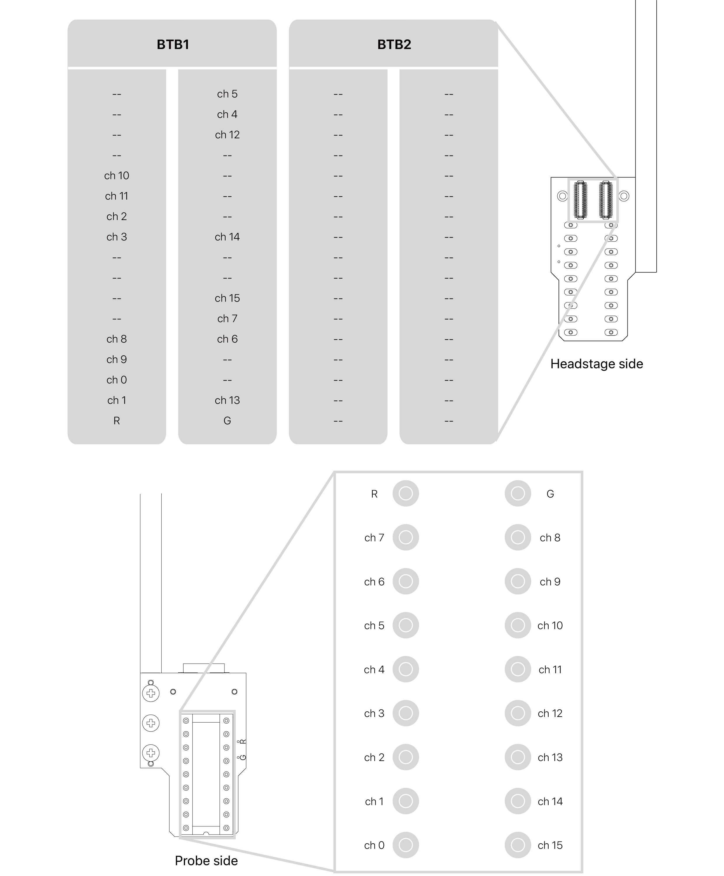
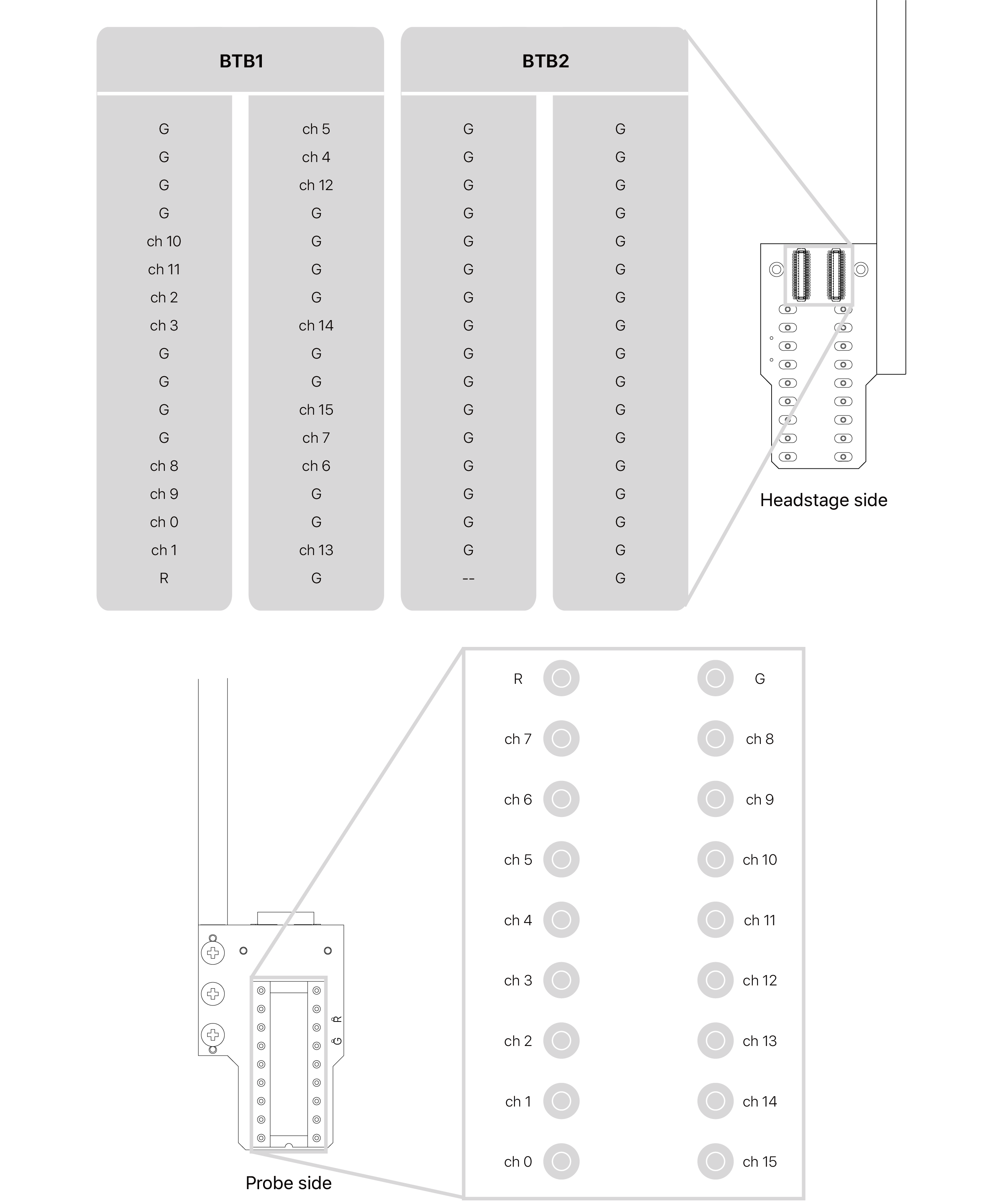
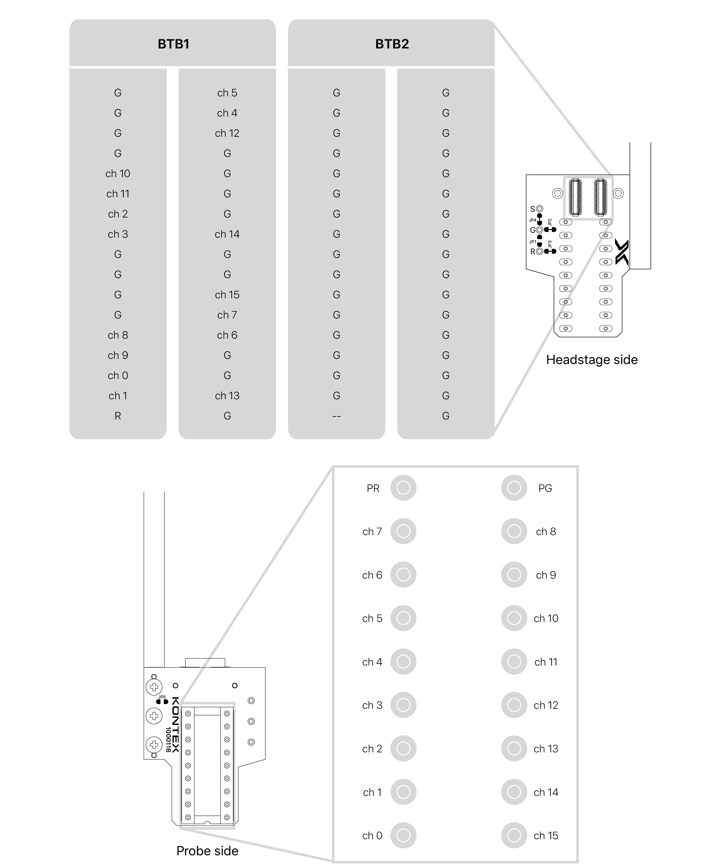
Pin Map
V1: Identified by K22022 on PCB
V1.1: Identified by 100011A on PCB
V2: Identified by 100011B on PCB
![]()