Adpt-OM16-V
Overview
The Adpt-Omnetics series is designed to interface KonteX X3(S)R headstages with probes using a support 16-, 32-, and 64-channel Omnetics connector's probe. Available in three configurations— standard with screw-locking for secure attachment, no-lock for a reduced footprint, and vertical to provide additional clearance near the craniotomy—these adapters enable flexible integration into diverse experimental setups while maintaining a compact and reliable connection.
Adpt-OM16-V Overview
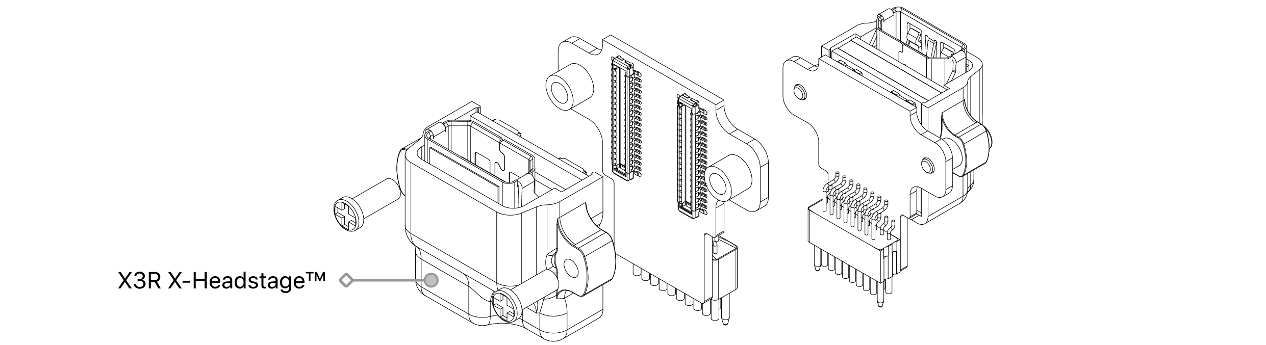
Adpt-OM16-V
Connector
- Molex PN: 505070-3422
- Omnetics PN: A79017-001
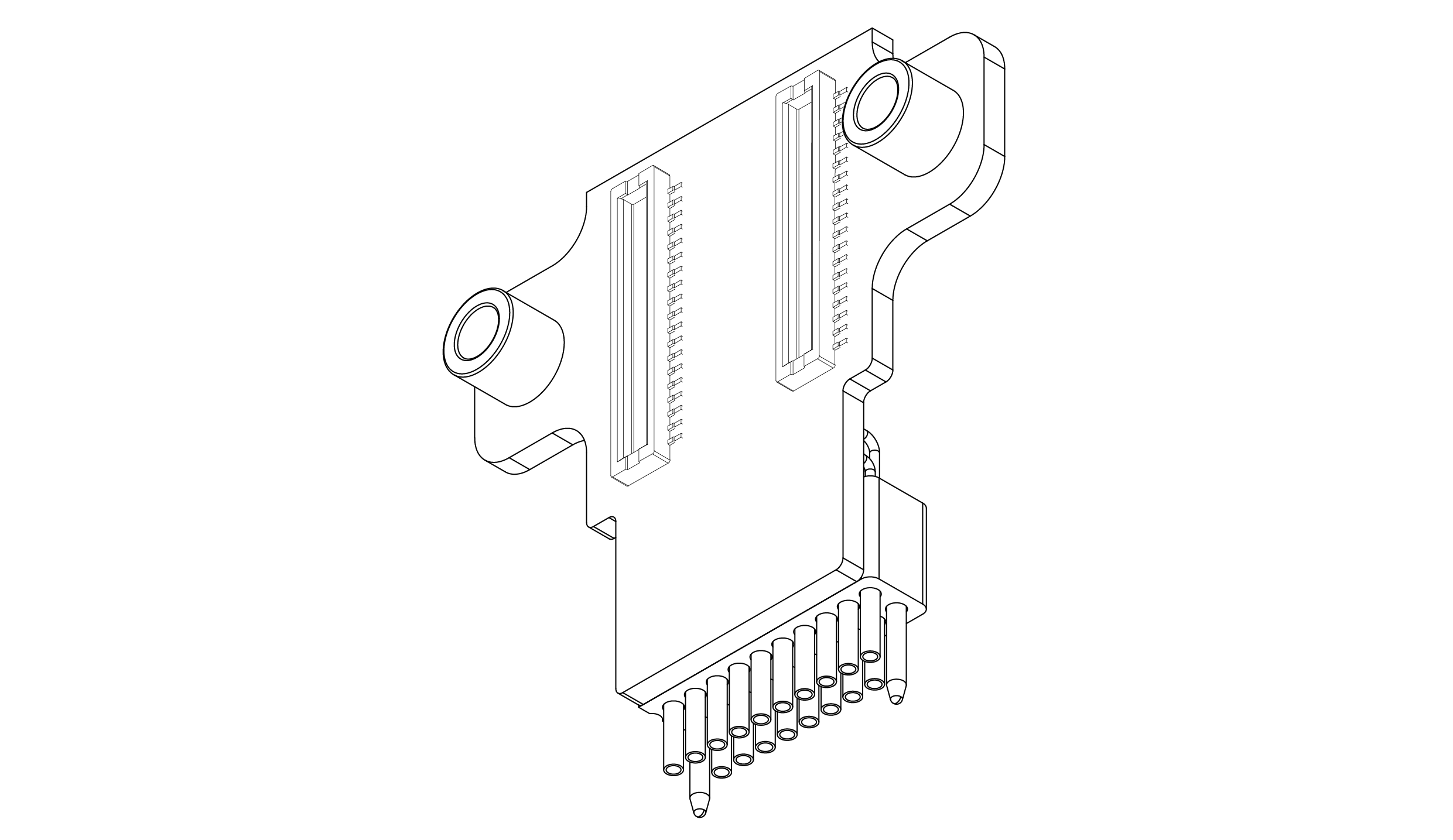
Headstage
Probe
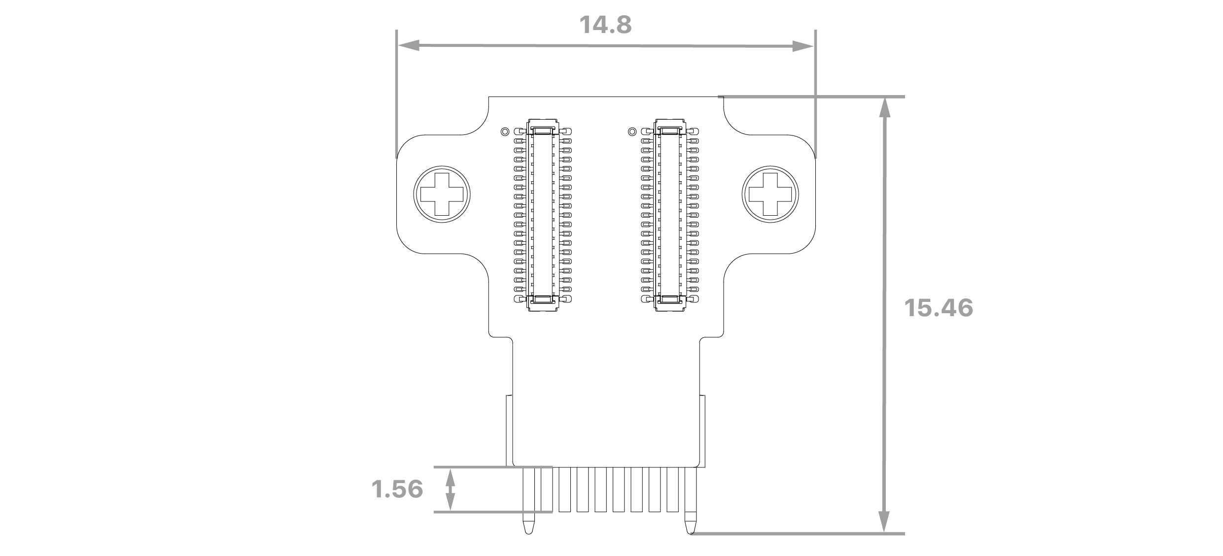
Dimension
OM16-V V1
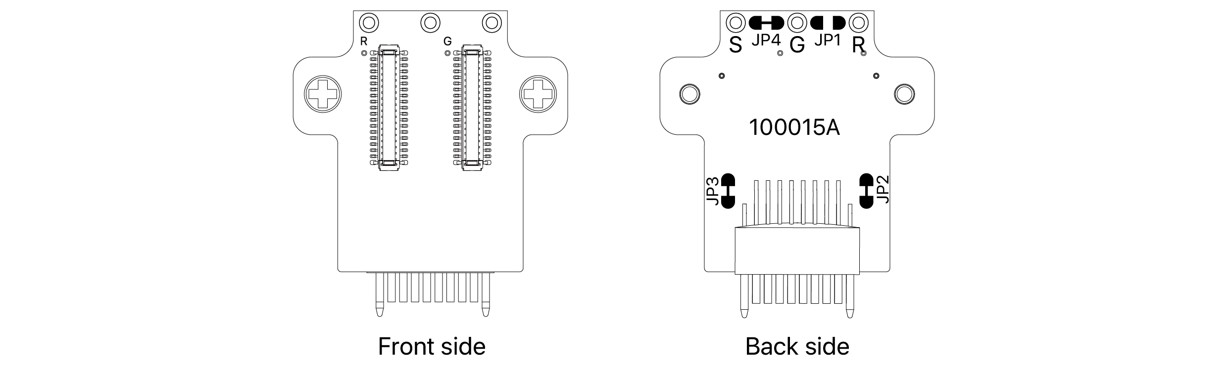
OM16-V V2
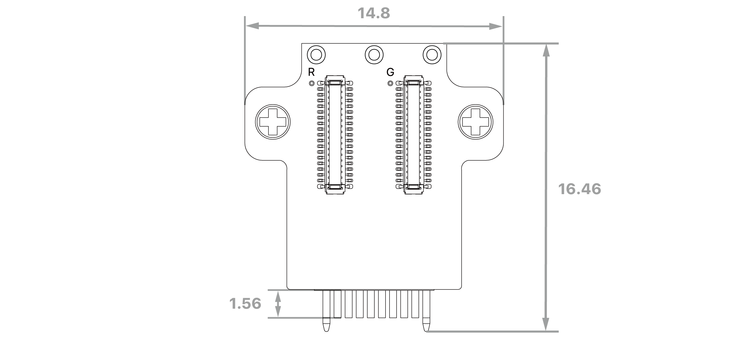
unit: mm
Versions
V1: Identified by PCB marking '100015' or by the blue board color when the marking is absent.
original design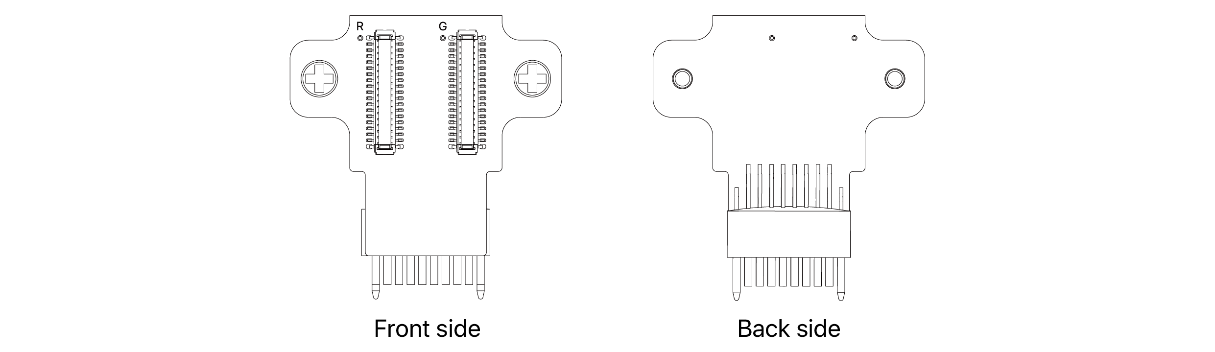
V2: Identified by 100015A on PCB
Ground & Reference Configuration
OM16-V V1 Adapter (SKU: Adpt-OM16-V v1)
- Ground (G) and reference (R) signals are independent by default.
- To short them together at the adapter, solder a short wire between the G and R pads.

Adpt-OM16-V
OM16-V V2 Adapter (SKU: Adpt-OM16-V v2)
Proper grounding and referencing are essential for high-quality signal acquisition. Always ensure that both ground and reference signals are securely connected. If either is left floating, significant noise may be introduced into the recordings.
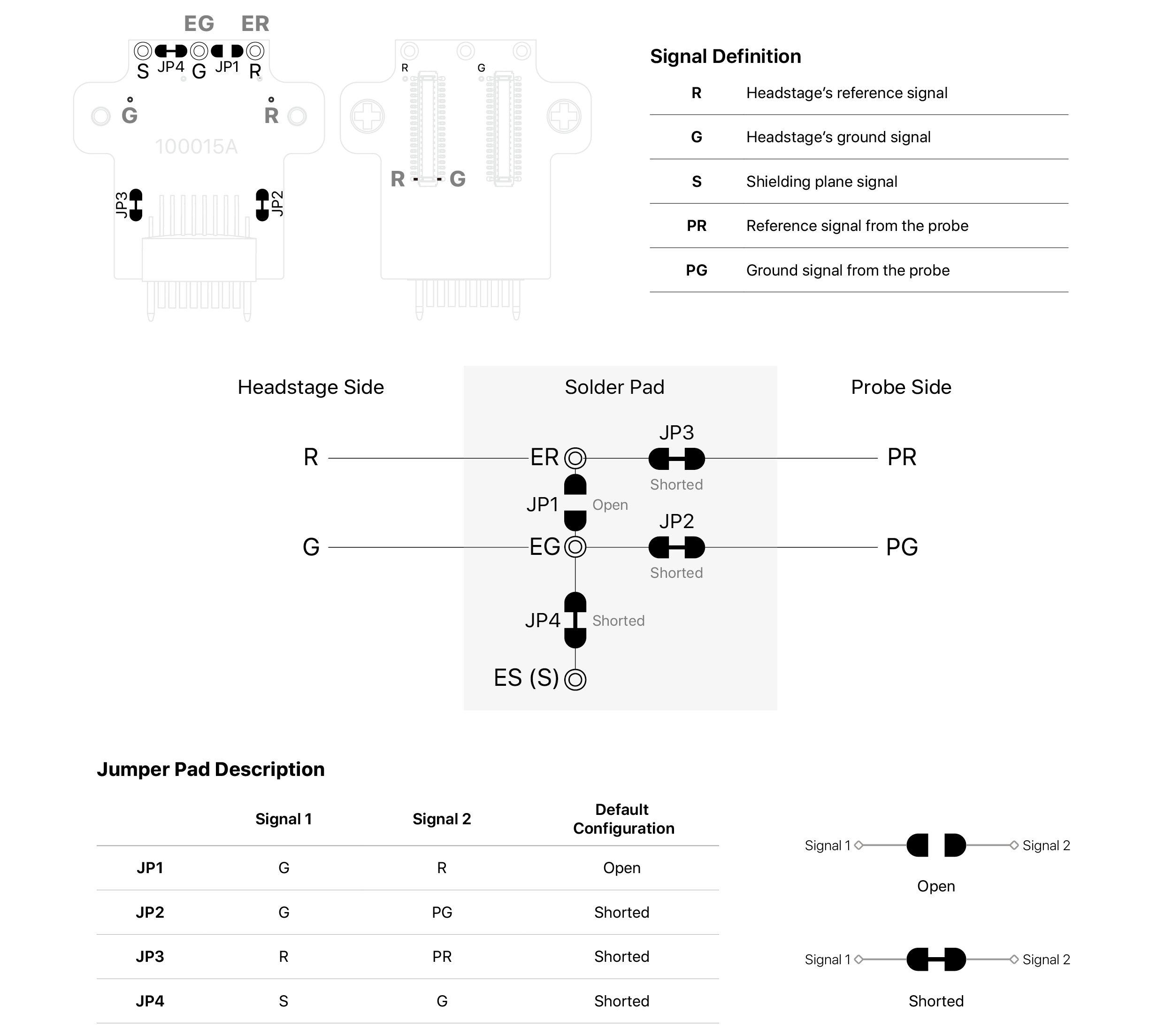
By default, the headstage ground (G) and reference (R) are independent.
- To connect reference and ground at the adapter, short JP1.
- Ground (G) is sourced from the probe ground (PG). To use an external ground (EG) via the adapter, cut JP2 and solder a wire to the EG pad.
- Reference (R) is sourced from the probe reference (PR). To use an external reference (ER) via the adapter, cut JP3 and solder a wire to the ER pad.
- Shielding (S) is connected by default to ground (G). To use an external shielding signal (ES) via the adapter, cut JP4 and solder a wire to the ES pad.
- The adapter’s metal rod is electrically isolated from the headstage. To connect it to the adapter’s shielding, short JP5.
Configuring the Jumper Pad
① To connect the jumper, apply solder around JP1 until a solid solder bead forms.

② To disconnect, use a soldering iron and desoldering mesh to remove the solder bridging the jumper pad.
If the jumper pas has a default short configuration, use a scalpel or precision blade to cleanly sever the trace.
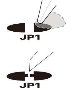
③ After modification, clean the area thoroughly using isopropyl alcohol or flux remover to eliminate any residual material.
④ Always verify connectivity using a multimeter to ensure proper configuration.
④ Always verify connectivity using a multimeter to ensure proper configuration.
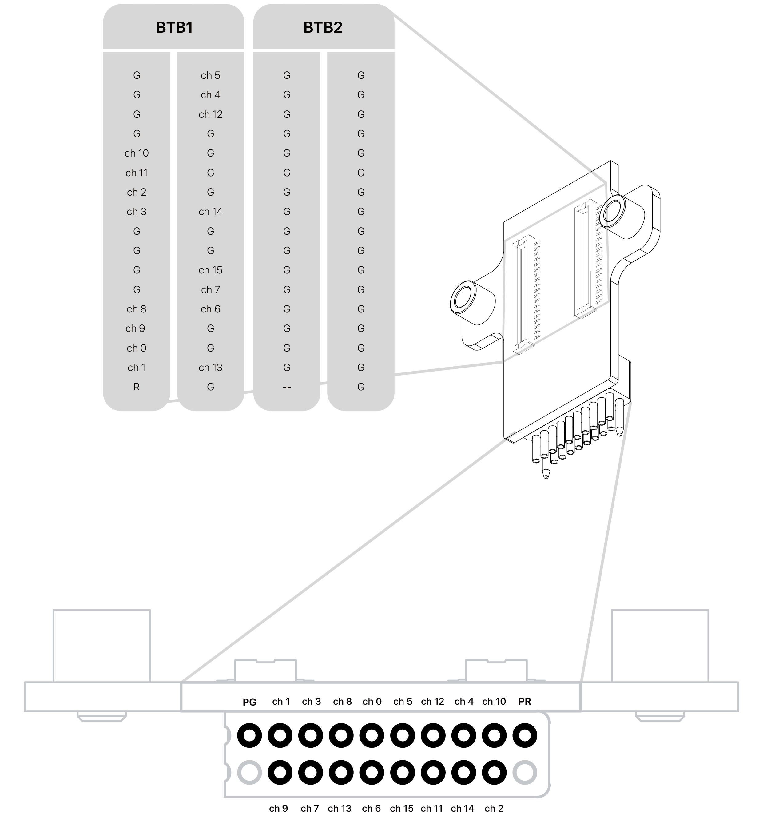
Pin Map
V1: Identified by PCB marking '100015' or by the blue board color when the marking is absent.

V2: Identified by 100015A on PCB
![]()